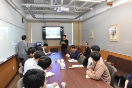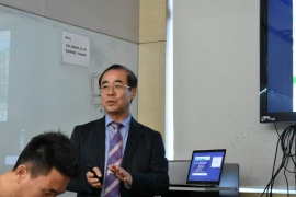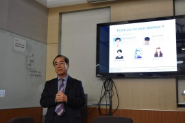
- Speaker: Prof. Eun Kyu Kim (Hanyang University)
- Date: Wednesday, October 17, 2018, at 17:00
- Place: Jungho Seminar Room
Among two-dimensional (2D) semiconducting layered materials, transition metal dichalcogenides (TMDs) such as MoS2 , WS2, and SnS2 with typical energy band gap of 1-2 eV have emerged as novel materials and have presented various fascinating physical properties. We
report a novel concept of nonvolatile memories utilizing functional van der Waals heterostructure in which multi-layered graphene is encapsulated between SiO2; and hexagonal boron nitride. It appeared that a large memory window (20 V) allows to reveal high on-/off-state ratio (>103 ). The devices with high charge storage capacity of few-layered graphene and high quality of WS2 manifest perfect retention of 13% charge loss after 10 years, which was recorded as 2 to 3 folds smaller than that of reported MoS2 memories. In recent, we studied also the hBN coupled SnS2 thin film transistors with bottom-gated device configuration. The electrical transport characteristics of the SnS2 channel transistor presents a high current on/off ratio, reaching as high as 105 and a ten-fold enhancement in subthreshold swing compared to a high-κ covered device. This structure showed the spectral photoresponsivity from ultraviolet to infrared in a multi-layered SnS2 phototransistor. These studies offer new device architecture for achieving future nanoelectronic building blocks by utilizing atomically thin van der Waals stacks.


